why are chips often so expensive? how do chip companies determine the prices of their chips? a thread...  https://abs.twimg.com/emoji/v2/... draggable="false" alt="🧵" title="Thread" aria-label="Emoji: Thread">
first thing chip companies do is to figure out the COGS - cost of goods sold. this is how much it costs them to produce a chip--not counting profit or anything else.
but before we can calculate that, we need to know The Life of a Chip, start to finish!
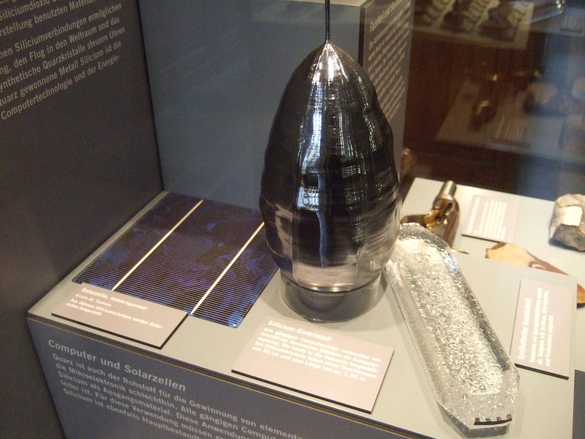
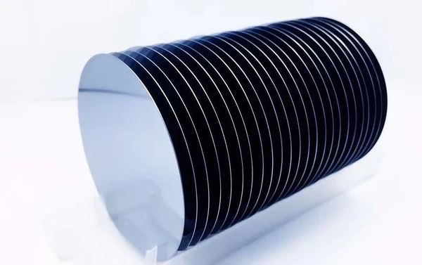
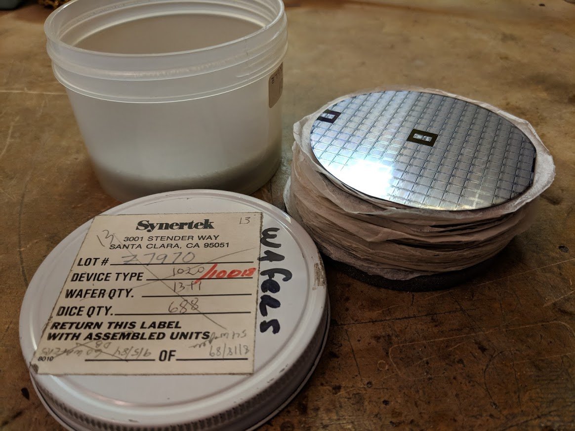
it starts as a raw slice of silicon, something like this. (0th step is a raw boule or silicon ingot, grown as a single crystal, that is sawn up like this)
then it gets run through a variety of processing steps. etching, diffusion, implantation, deposition, and others.
after the wafer is done, it goes through a process called "wafer sort" where each chip is measured and tested, and the bad ones are marked electronically. in the old days they used a drop of red ink.
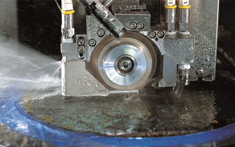
the next step is to cut apart the wafer into separate squares of silicon. this is called "singulation" and it is done with a diamond saw.
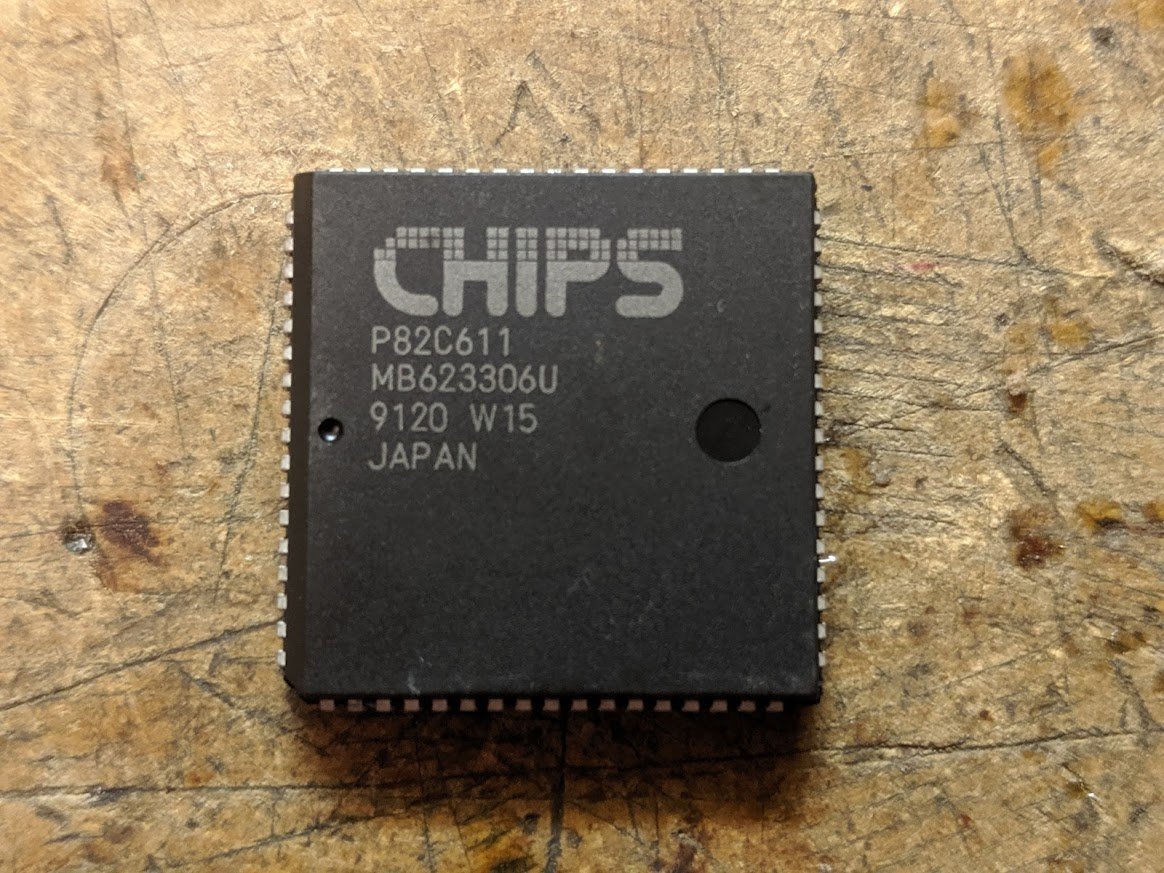
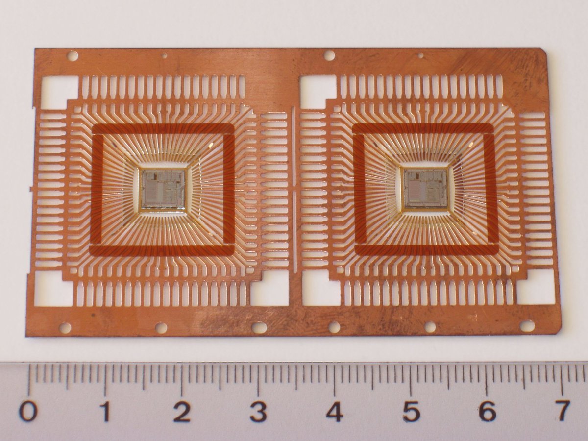
the individual die are then sealed inside a package and marked with the part number and manufacturer logo. at this point it is recognizable as a chip.
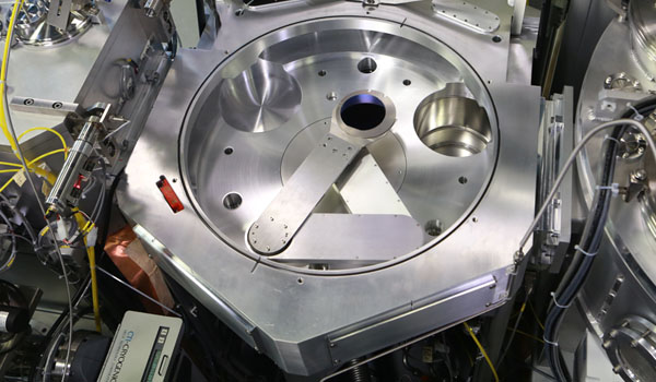
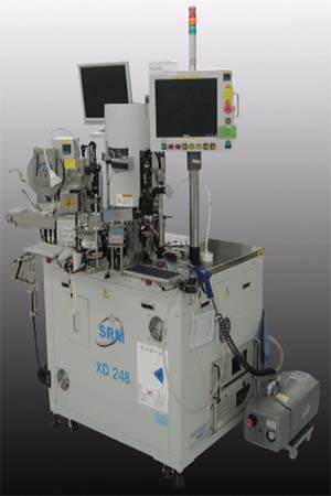
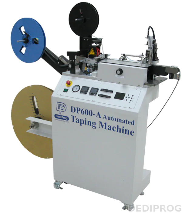
this packaged chip might have been damaged during singulation or packaging, so it has to be tested again. this is called "final test". it goes into a machine that looks something like this, and all the critical parameters are measured.
in the last step, tested good chips get loaded into trays, tubes, or reels, packaged up, labelled, and shipped off to customers or distributors.
all right--back to cost. the first big number is the cost of a processed wafer. this is the wafer after all the semiconductor processing steps have been applied.
the cost of a wafer depends on the semiconductor process, the wafer size, facility costs, labor involved, materials, etc. even though the raw wafer costs around $100, a processed wafer can cost between $500 and $2000 or even more!
wafer costs are often measured using the concept of a "financial move" -- a single process step that costs money. this could be mask+etch, diffusion, deposition, etc.
a simple process might have around 100 financial moves. complex processes have 200-300 moves or even more!
certain features require financial moves. for example, if you have a neat microcontroller but you want to add embedded flash memory, that& #39;s about 25 financial moves. the wafer cost goes up!
we also can& #39;t forget NRE (non-recoverable expenses). these are things you have to pay for *once* per chip design. a very large expense is the mask set.
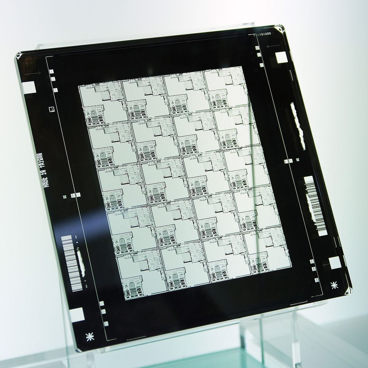
a mask contains a very precise set of images that form connective wiring and other features on a chip. masks are part of the photolithography process that transfers the pattern to the surface of the silicon.
mask sets (since a chip requires many, many masks!) can cost a huge amount. for example, the mask set for a single design in a 28nm process costs around 3 million dollars!
if you& #39;re an IC designer, you also want to leave little hooks in the design so that you can fix bugs by changing as few masks as possible. you don& #39;t want to pay for a brand new mask set if you screw something up!
typically NRE is accounted for separately. for this discussion i& #39;m focusing on the unit cost.
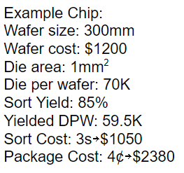
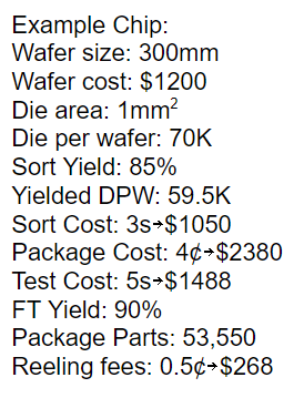
to figure out how much a single die costs, we first have to figure out how many die we can fit on a wafer. for example, with a 300mm wafer and a die area of 1mm2, you can fit about 70,000 die on a single wafer.
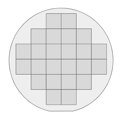
this formula doesn& #39;t work for really large die sizes, since the die in the corners are incomplete and have to be thrown away. round peg, square hole.
but not all of the chips on the wafer will work, so we have to throw those away after we test the wafer at wafer sort.
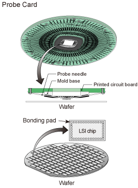
for wafer sort, we have another NRE: the probe card. this has probes permanently positioned to touch the bond pads on the die.
for wafer sort, we have another NRE: the probe card. this has probes permanently positioned to touch the bond pads on the die.
the percentage of parts that pass the test is our "sort yield." so if we have 70K parts going in and our sort yield is 85%, then we get 59,500 working die and the rest are bad and have to get thrown out.
this wafer sort process costs money, too! about a half cent per second per part is a good rule of thumb. so a complex part that takes longer to test will cost more to test. oh and in our example, you have to test all 70K parts since you don& #39;t know which ones are bad yet!
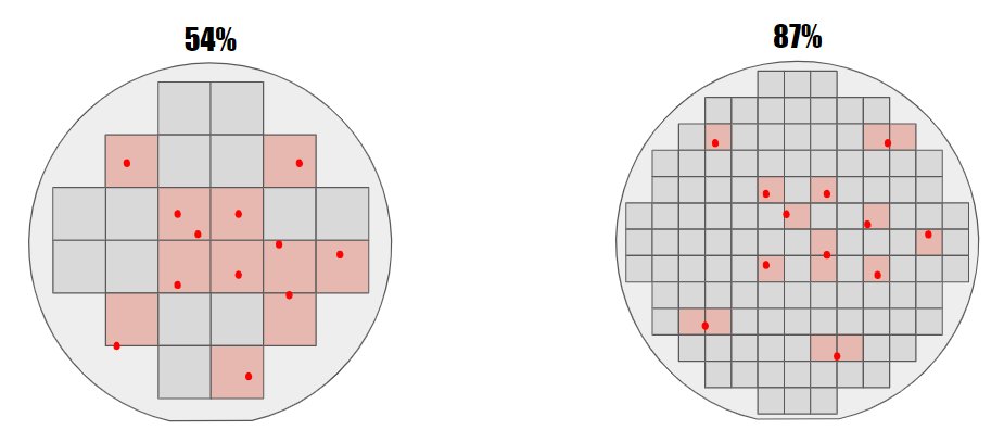
there are a variety of reasons why die don& #39;t work on a wafer. usually this is all lumped together into a "defect density" that is tied to the process.
processes with a high defect density aren& #39;t totally useless but they& #39;re bad for larger chips. here are two wafers with the same defects, and you can visually see how the yield is much better for a smaller die size.
ok, now we singulate the wafer and put each part in an IC package. this, naturally, costs money. the exact number depends on the package.
for example, we could use an old standby, the 8-pin SOIC. this costs less than a cent. it& #39;s cheap, it& #39;s kinda big, but it does the job. a QFN package is smaller and has better thermal characteristics, but it can cost between 3 and 15 cents depending on the size and pin count.
DIP packages are now more expensive than surface mount since they& #39;re in less demand. then there are exotics like ceramic and metal, and those can get *really* expensive.
then there are a variety of flip-chip packages. they have little solder bumps that are applied to the whole wafer all at once. this usually costs around $150 to $200. if we did this for our example wafer, that would cost around 3 cents.
here& #39;s the running tally for our example chip.
now we get to final test. this step, besides testing each chip, can also do things like trim voltage references. the stress of being inside a plastic package causes them to shift in voltage, so you have to compensate for that.
how much will that cost us? well, if we test only at room temperature, it& #39;s just a fraction of a cent per second! 0.2 to 0.5, depending on the equipment you& #39;re using, facility, labor, etc. the more parameters to test, the longer it takes!
oh, and if you need to test at high temperatures as well so that you can guarantee some critical analog spec, then double that cost! if you also need to test at low temperatures, double it again!
if you need to do fancy things like binning or laser marking, then that costs money as well.
there& #39;s another yield number called "final test yield" which means we throw away bad parts. for our example, let& #39;s say we have a 90% FT yield. we now have 53,550 working parts. and if our test time was around 5 seconds, that process cost us $1488.
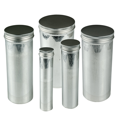
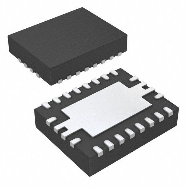
but these parts are in a metal can, like one of these. customers want to load them into a pick-and-place machine, so they want them on a reel or in a tray.
now let& #39;s figure the grand total for our example. we have spent $6386 and we& #39;ve gotten back 53,550 tested parts that are packed up and ready to go to the customers. so our cost is 11.9 cents per part.
but that& #39;s not what the customers pay! we have to charge extra so that we can pay our engineers, creditors, facilities, and shareholders. the price we charge the customer also depends on the size of the order. usually there& #39;s a rule of thumb to use for gross margin.
for really high volume customers, 50% margin or even less is fairly common. but for smaller customers who don& #39;t buy many parts, the gross margin goes to 80% or even more.
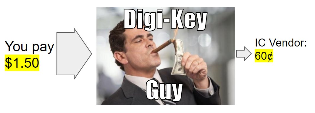
for our example chip, 80% gross margin would mean that the customer pays 60 cents for a part that cost us 11.9 cents to produce.
if the part gets sold through a distributor, they have a special pricing strategy  https://abs.twimg.com/emoji/v2/... draggable="false" alt="😂" title="Gesicht mit Freudentränen" aria-label="Emoji: Gesicht mit Freudentränen">
back when i worked in the business, i used to define new products. it& #39;s basically technical marketing. one of the skills that i had was being able to quickly estimate how much a hypothetical part would cost.
example: a process costs 3 cents per mm2. a part might be 4x4mm, so die cost is 48 cents. 8x8 QFN package is maybe 15 cents, test time is 10 seconds, so test is 5 cents. total cost is around 68 cents, and with 50% margin we double that to get $1.36 price for high volume customers
chip companies also figure out little tricks they can do to save money in clever ways. for example, for doing flip chip, you can bump *before* wafer sort and then wafer sort becomes your final test. that saves a whole step!
other companies have little barriers to competition that they erect. Linear Tech likes to put all their parts in non-square QFN packages. they negotiate a good price, but their competitors rarely use the packages and have to pay a premium, making them less able to compete.
not all parts are worth spending the money and time to develop. part of the product definer job is figuring out if a part is worthwhile, and naturally there& #39;s a formula for that!
it& #39;s called RODT  https://abs.twimg.com/emoji/v2/... draggable="false" alt="🐀" title="Ratte" aria-label="Emoji: Ratte"> which stands for Return On Design Time.
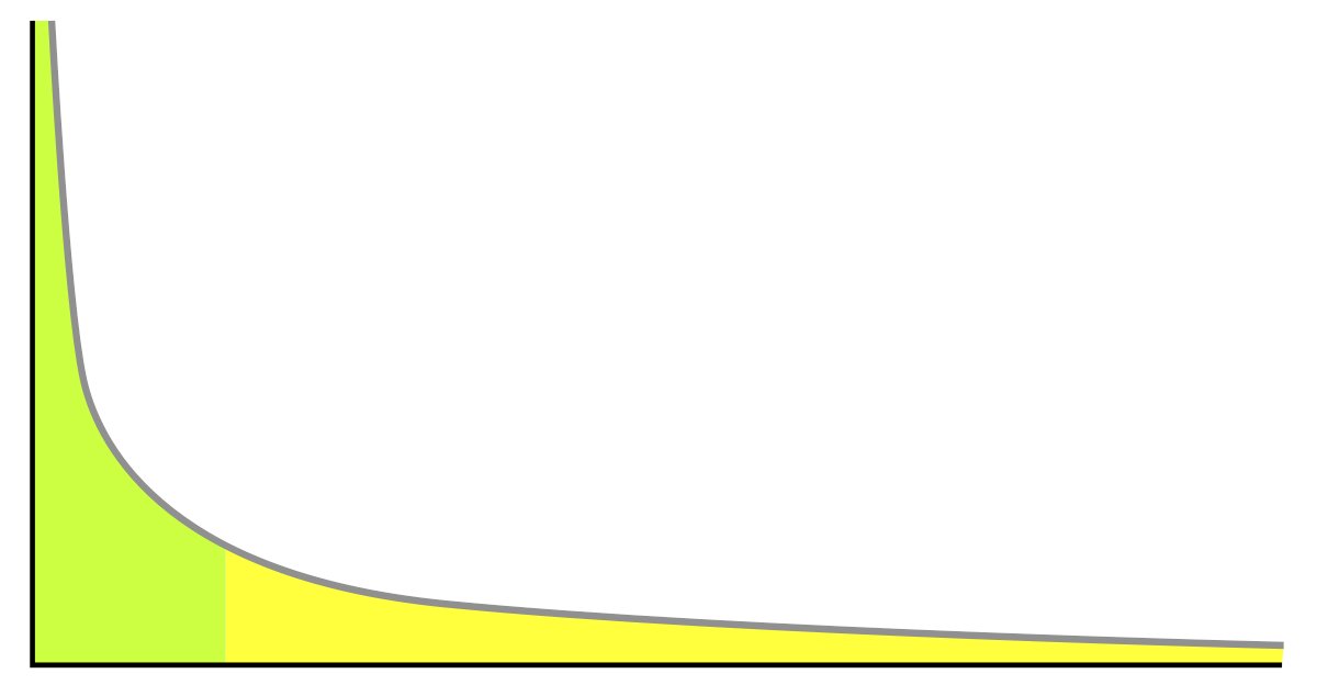
it& #39;s definitely got limitations. you have to figure out how long you& #39;re going to sell the product. don& #39;t underestimate the long tail!
you& #39;ve also got to account for product support costs in addition to design time. i& #39;ve seen products fail because they were too complex and very costly to support. apps engineers aren& #39;t free, and complex parts involve lots of interaction with customers.
for further reading, i& #39;d suggest "Microchip Fabrication" by Peter Van Zant. you could also read a business finance book but watch out as this path leads to the dark side.  https://abs.twimg.com/emoji/v2/... draggable="false" alt="😜" title="Winking face with tongue" aria-label="Emoji: Winking face with tongue">
some people were asking about a certain Cupertino fruit company. they typically don& #39;t pay for chips in the traditional way. they hired a bunch of folks out of that industry, and they will take your chip and figure out exactly how much it costs you to make.
it& #39;s basically the square area of the chip. so they take your chip, figure out the square area, apply their little formula, and that is what they pay you. don& #39;t like it? too bad, they just go to your competitor.
technical issues crop up over a holiday weekend? too bad, you have to respond and have a team over there in a few hours.
people get all excited about their in-house silicon. another, more cynical take: they& #39;ve burned so many chip companies over the years that they pretty much have no other choice. but they have to be nice to their fabs because there& #39;s only hmm ~3 of them in the world.
people are commenting about process nodes. part of the art of product definition is being able to judge what process a part should go into.
if you have a fairly simple part and a really small process, you could become "pad limited" where the die size is limited by the size of the pads. this means you& #39;re paying for an expensive wafer and you& #39;re not using it for active circuitry. lots of empty areas.
someone asked about those 5c microcontrollers from China. how do they do it? lots and lots of die per wafer on a commodity (reasonably small) process. cheap packages. wide open specs. minimal testing.
another good trick: skipping wafer sort (called "blind build") and just packaging up *all* the parts can sometimes save money if your wafer sort yield is really high and you don& #39;t need to do any trimming steps.
in the old days, you couldn& #39;t skip it because trimming (adjusting reference voltages, offsets, etc) had to be done with a laser, and you can& #39;t do that with a package in the way. nowadays we have OTP (one-time program) memory so that can all get done after packaging.
it& #39;s so strange to me that wall street seems to consider the chip business to be in "harvest mode" when there are constantly new and interesting product lines coming up. there& #39;s still a ton of innovation going on!
i mean at one level yes you could consider silicon to be fungible. but at another level, there& #39;s a big difference in the actual circuits to be found on a chip!
it& #39;s like evaluating hollywood studios by how many feet of film they produce in a year
or a candy company by how many feet of fruit--wait
but even processes aren& #39;t all interchangeable. maybe for digital, but good analog processes give designers a balanced set of tools for making high quality parts.
although you can get away with some ridiculous things like making dirt cheap op amps using a crappy digital process and trimming the crap out of it to compensate for process variation. but even that is innovative.
before i forget, i also want to correct a mistake: i called NRE "non-recoverable expenses" but it should be "non-recurring expenses."
some people asked why wafers are round. they are grown from a single crystal of silicon in a vat and they come out that way.
(diagram shows germanium boule, but silicon is the same way)

 Read on Twitter
 " title="why are chips often so expensive? how do chip companies determine the prices of their chips? a thread... https://abs.twimg.com/emoji/v2/... draggable="false" alt="🧵" title="Thread" aria-label="Emoji: Thread">" class="img-responsive" style="max-width:100%;"/>




 " title="if the part gets sold through a distributor, they have a special pricing strategy https://abs.twimg.com/emoji/v2/... draggable="false" alt="😂" title="Gesicht mit Freudentränen" aria-label="Emoji: Gesicht mit Freudentränen">" class="img-responsive" style="max-width:100%;"/>
 which stands for Return On Design Time." title="it& #39;s called RODT https://abs.twimg.com/emoji/v2/... draggable="false" alt="🐀" title="Ratte" aria-label="Emoji: Ratte"> which stands for Return On Design Time." class="img-responsive" style="max-width:100%;"/>
