I recently read a fascinating paper from 1962 on the detailed history of how the transistor was invented.
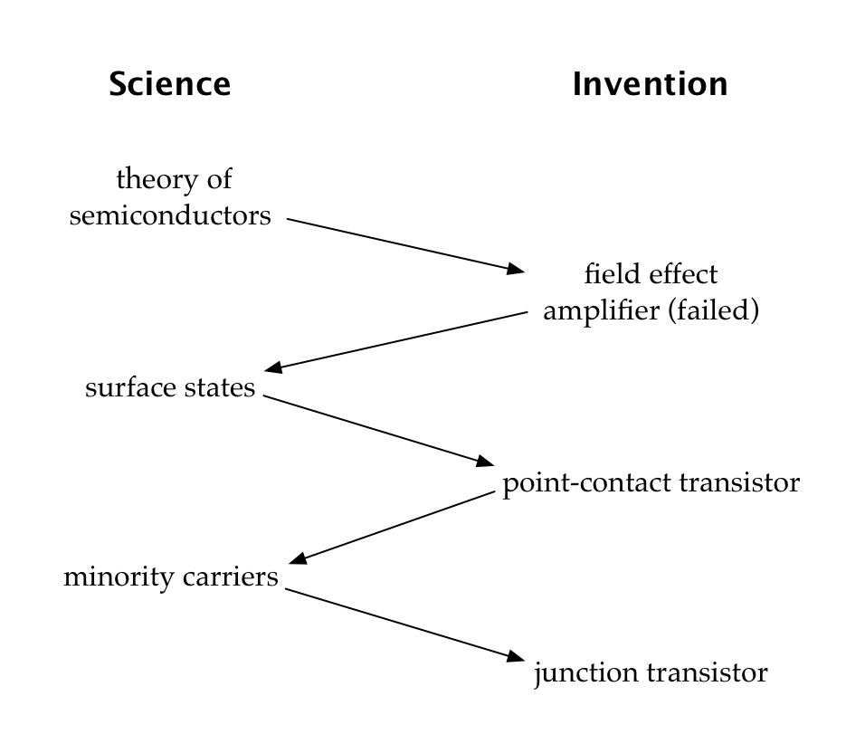
What stood out was how the researchers cycled back and forth between science and engineering.
What stood out was how the researchers cycled back and forth between science and engineering.
The semiconductor group at Bell Labs was set up after WW2. They didn& #39;t know exactly what they could invent, but they felt the time was ripe for a major breakthrough. Semiconductor physics had come a long way, and a theoretical basis had been laid out in the 1930s.
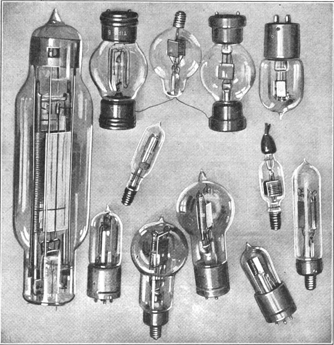
Among various possibilities was that of a solid-state amplifier. The vacuum tube amplifier was invented by inserting a metal grid into a vacuum tube rectifier. Semiconductors could also rectify—maybe with modification, they could amplify?
They tried the same trick: insert a metal grid. Didn& #39;t work.
Then they tried using an electric field instead of a grid, a concept called a field effect amplifier. Shockley validated the idea with calculations based on a theoretical model.
Then they tried using an electric field instead of a grid, a concept called a field effect amplifier. Shockley validated the idea with calculations based on a theoretical model.
But what worked in theory failed in experiment. Sometimes the effect was orders of magnitude smaller than predicted; sometimes it was *backwards*.
To explain the failure Bardeen proposed a new theory: that electrons were trapped in “surface states”.
To explain the failure Bardeen proposed a new theory: that electrons were trapped in “surface states”.
Based on the new theory, they began experimenting to find a way to neutralize the surface states and so to make a working field effect amplifier.
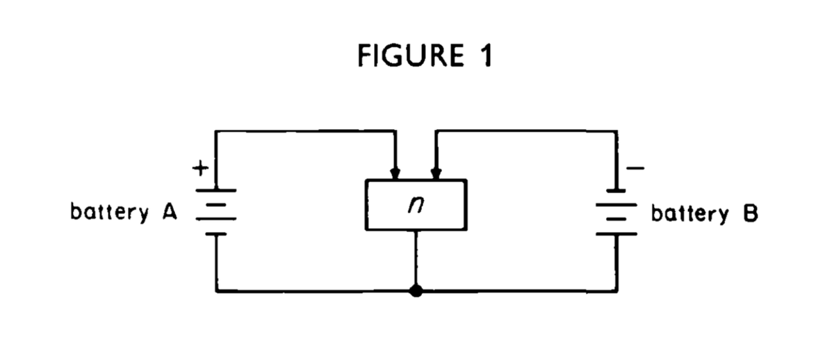
In one of their experiments, they put two contacts close together on a piece of n-type semiconductor:
In one of their experiments, they put two contacts close together on a piece of n-type semiconductor:
What they discovered was an amplification effect! This was *not* what they were expecting—but it was, of course, what they were ultimately looking for.
So now they had a potential solid-state amplifier—later termed a transistor. But why did it work?
So now they had a potential solid-state amplifier—later termed a transistor. But why did it work?
Back to theory.
It was known that n-type semiconductors have an excess of electrons, which flow through the material to carry a charge. P-type material has an excess of “holes” where electrons could be but aren& #39;t. As electrons jump backwards, these holes “move” forwards.
It was known that n-type semiconductors have an excess of electrons, which flow through the material to carry a charge. P-type material has an excess of “holes” where electrons could be but aren& #39;t. As electrons jump backwards, these holes “move” forwards.
What wasn& #39;t appreciated was that electrons can also flow through p regions, and holes can flow through n regions. These are called “minority carriers.”
Minority carriers explained the experiment: holes were flowing between the two contacts. But there was more—
Minority carriers explained the experiment: holes were flowing between the two contacts. But there was more—
The idea of minority carriers also allowed Shockley to theorize an improved transistor design: the junction transistor. In an n-p-n junction transistor, a thin slice of p-type material is wedged between two n regions. When a voltage is applied, current flows through the p region.
So the Bell Labs researchers shuttled back and forth between engineering and science, between discovery and invention. Unexpected results—whether disappointing or exciting—sent them back to theory; new theory reinvigorated experiment.
And it& #39;s unclear if the transistor could have been invented any other way, at the time. Key ideas in semiconductor physics, surface states and minority carriers, were missing or insufficiently developed.
To run a lab like this requires researchers who are trained in, and motivated by, both science and invention. And it requires management that is open to both, and that gives researchers the freedom to quickly pivot between them and among various approaches.
Do our current models of funding, organizing and managing research support this mode?
Elaboration on this thread in the full blog post version: https://rootsofprogress.org/transistors-science-and-invention">https://rootsofprogress.org/transisto...
And if you like this kind of stuff, subscribe to @rootsofprogress: https://rootsofprogress.org/subscribe ">https://rootsofprogress.org/subscribe...
The paper is “The Link Between Science and Invention: The Case of the Transistor”, Richard Nelson, 1962: https://www.nber.org/chapters/c2141
The">https://www.nber.org/chapters/... figures above are from the paper. Images above are from @WikiCommons and are public domain. Zig-zag diagram created by me.
The">https://www.nber.org/chapters/... figures above are from the paper. Images above are from @WikiCommons and are public domain. Zig-zag diagram created by me.

 Read on Twitter


